Voltage source inverter (VSI) interface#
This chapter documents the voltage source inverter (VSI) interface at the software level. For the physical-level description involving the specific signal names, signal levels, dynamic range, impedance, etc., refer to the hardware-specific datasheets.
Interface signals#
The interface between Telega and the voltage source inverter consists of several analog and discrete signals summarized in the following diagram.

VSI model used in Telega and its interface signals.#
Configuration registers#
The default values are heavily dependent on the kind of product; therefore, they are not shown here.
Register |
Type |
Unit |
Description |
|---|---|---|---|
|
|
\(f_\text{PWM} = f_\text{tick}\times{}2^x\), where \(x\) is the parameter value. |
|
|
|
second |
PWM dead time modulated at the bridge gate outputs (additional dead time may be added by the hardware). |
|
|
1 |
Ratio of the DC link voltage to the sensing pin voltage. |
|
|
\(\frac\A\V\) |
Ratio of the phase current to the sensing pin voltages, per gain level. |
|
|
ampere |
Standard error of the phase current measurement circuit, per gain level. |
|
|
second |
Phase current gain increase (reduction of amplification) delay. |
|
|
volt |
Phase current gain reduction/increase thresholds, expressed as voltages at the sensing pins. |
|
|
ohm |
Total 3-phase bridge resistance per arm (incl. current shunts, if any): \(A_H, A_L, B_H, B_L, C_H, C_L\). |
|
|
second |
Time from the enable signal assertion to the moment when the VSI is operational. |
|
|
second |
Do not permit the enable signal to remain deasserted for a shorter amount of time than this. |
|
|
second |
Keep all phases grounded for this amount of time while sampling the phase currents. |
|
|
second |
Ignore hardware fault signal pulses shorter than this. |
|
|
second |
The total amount of time to collect samples during the calibration process. |
|
|
\(\K, \frac\K\V, \frac\K{\V^2}\) |
Thermistor polynomial coefficients. |
|
|
If set, phases A and B are swapped. |
Three-phase bridge control#
Telega generates three complementary PWM signals driving the six-switch three-phase bridge.
Telega can insert dead time configurable via vsi.pwm_dead_time.
The bridge driver circuitry can extend the dead time modulated by Telega dynamically as necessary,
e.g., using an automatic dead time control circuit.
With some smart driver ICs (e.g., TI DRV8xxx),
the explicit dead time insertion by Telega can be disabled completely (by setting the register to zero)
to fully delegate this concern to the hardware,
as Telega does not require the knowledge of the actual dead time observed on the bridge.
Telega provides an enable signal that indicates whether the power stage hardware shall be in the operational state or in the disabled, low power consumption state. In the standby and fault states, the enable signal is always deasserted. The hardware can leverage this signal to control the activation of the components of the inverter (e.g., power supply, amplifiers, etc.).
It is recognized that the inverter circuitry may be unable to enter the operational state immediately when
the enable signal is asserted.
The vsi.activation_latency parameter specifies the amount of time that must be allocated to the VSI
to transition from the disabled state to the enabled state, where it is ready for normal operation.
Certain smart driver ICs have a hardware defect that may cause the IC to enter an invalid state
if the enable signal is briefly deasserted and then asserted again shortly afterwards.
A work-around is available via vsi.shortest_time_in_disabled_state,
which instructs Telega to hold the enable signal deasserted for at least the specified amount of time
before asserting it again.
System tick and PWM frequency#
The system tick phase is aligned to the PWM phase;
the integer ratio between the PWM frequency and the system tick frequency is configurable
via vsi.pwm_freq_mul_log2 as \(f_\text{PWM} = f_\text{tick}\times{}2^x\), where \(x\) is the parameter value.
This enhances the compatibility of Telega with low-inductance motors (e.g., coreless) where a higher switching
frequency is desired but increasing the tick rate is not possible due to performance limitations.
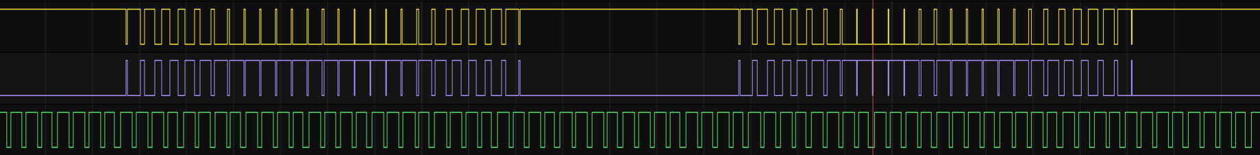
Oscillogram of PWM signals \(A_L\), \(A_H\), and the system tick execution indicator with a multiplier of 1.#
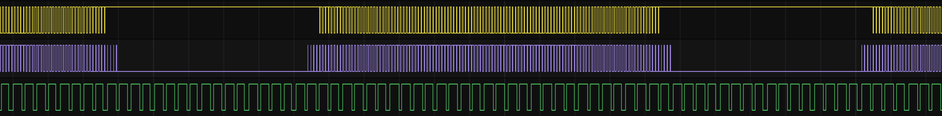
Oscillogram of PWM signals \(A_L\), \(A_H\), and the system tick execution indicator with a multiplier of 4.#
DC voltage measurement#
The DC voltage \(u_\text{dc}\) is measured through an analog voltage input pin,
whose voltage \(\hat{u}_\text{dc}\) is a function of the DC link voltage as
\(u_\text{dc} = \hat{u}_\text{dc}\,x\),
where \(x\) is the value of vsi.dc_voltage_gain.
The measurement circuit is often implemented as a simple resistive voltage divider,
in which case \(x = \frac{R_L+R_H}{R_L}\).
The low-pass cutoff frequency of the DC sensing circuit should be less than half of the tick frequency and not lower than 1 kHz.
DC current measurement#
Telega does not measure the DC current directly, as this parameter is not required for motor control. Instead, this value is predicted from the AC system quantities. The DC link current estimates are expected to exhibit a large error when the drive is unloaded, and converge to the minimum at the maximum phase current amplitude.
Phase voltage measurement#
The phase voltage measurement inputs \(\hat{u}_{abc}\) are discrete inputs, where for phase \(x\), the input signal is a function of the phase voltage as \(\hat{u}_x = u_x \gtrapprox{} \frac{u_\text{dc}}{2}\).
The phase voltage feedback circuit is highly sensitive to the signal propagation delay and its symmetry. For optimal performance, it is recommended to ensure that the propagation delay does not exceed 50 ns, and the leading/trailing front asymmetry does not exceed \(\pm{}5\) ns. This deserves special attention if galvanic isolation is used. Refer to the hardware-specific documentation for additional information.

A possible implementation of the phase voltage measurement circuit.#
Phase current inputs#
Transfer function#
There are two approaches to the phase current measurement, both of which are supported by Telega:
In-line — the current is measured directly at the motor phases. This is commonly implemented with current shunts with isolated amplifiers or Hall sensors. This method is technically superior but is often more complex and expensive to implement.
Low-side — the current is measured between the ground and low-side switches using shunt resistors, as shown in the diagram. This method has limitations explored in the Sampling window section, but it is usually easier to implement.

Low-side current sensing schematic. Notice the polarity of the amplifier connection.#
The phase current measurement inputs \(\hat{i}_{abc}\) are analog voltage inputs,
whose voltage is a linear function of the phase current and the selected scalar gain \(G_i\)
\(\left[\frac{\text{ampere}}{\text{volt}}\right]\): \(i_{abc} = \hat{i}_{abc} \, G_i\).
The gain \(G_i\) is specified via vsi.phase_current_gain, more on this in the following section.
Telega is invariant to the method of current measurement used (shunt resistors, Hall sensors, in-line, low-side, etc.) as long as the transfer function of the sensing circuit is expressible in terms of the above model.
By convention, the measured current value is positive when the phase current flows from the inverter into the motor, and vice versa.
Depending on the hardware, current sensing on phase C may not be available; in which case, it is deduced from the other two.
Automatic gain control (AGC)#
Telega supports four selectable gain levels managed by the AGC algorithm. The currently active gain level is communicated to the VSI via two discrete outputs as follows:
Gain level |
Output 1 (MSb) |
Output 0 (LSb) |
\(G_i\) value |
Analog amplification |
Current magnitude |
|---|---|---|---|---|---|
0 |
0 |
0 |
High |
Low |
High |
1 |
0 |
1 |
|||
2 |
1 |
0 |
|||
3 |
1 |
1 |
Low |
High |
Low |
When the state of the gain selection outputs is changed, the hardware shall reconfigure the amplifiers and the transients shall settle in less than one system tick period.
The gain levels are specified via vsi.phase_current_gain, each level at its index;
i.e., the high-current, low-amplification gain level is at index 0.
The switching thresholds \(x_H\) and \(x_L\) [volt] are set via vsi.phase_current_gain_attack_decay, respectively.
The AGC algorithm utilizes them as follows:
Attack condition: \(G_i\) is increased (i.e., analog amplification reduced) immediately when \(\max(|\hat{i}_a|, |\hat{i}_b|, |\hat{i}_c|) \ge x_H\)
Decay condition: \(G_i\) is reduced (i.e., analog amplification increased) if the following is observed for
vsi.phase_current_gain_decay_timeseconds continuously: \(\max(|\hat{i}_a|, |\hat{i}_b|, |\hat{i}_c|) < x_L\)
Incorrectly chosen switching thresholds may lead to saturation, signal distortion, and/or gain oscillation. To avoid these issues, the choice of thresholds needs to satisfy the following conditions:
\(x_H\) shall be within the linear region of the amplifiers (as observed at the output). Otherwise, the amplifiers will enter the non-linear region before the gain adjustment takes place, thereby distorting the signal.
\(x_H\) shall be within the dynamic range of the ADC (for a single-ended ADC, this is half of the reference voltage). Otherwise, the ADC will enter saturation before the gain adjustment takes place, thereby clipping the signal.
Ratio \(\frac{x_H}{x_L}\) shall be strictly larger than the largest ratio of any two adjacent gain levels. Otherwise, gain oscillation will take place.
If the hardware only supports two gain levels, then:
Only gain levels #0 and #2 should be used.
Level #1 should be configured identically to #0.
Level #3 should be configured identically to #2.
Output 0 should be left unconnected.
If the hardware supports only one gain level (i.e., no dynamic gain control), then all gain levels should be configured identically.
As the current measurement circuit may exhibit different signal-to-noise ratios, depending on the selected gain level,
the standard error (square root of the error variance)
is specified separately per gain level via vsi.phase_current_stderr.
The standard error value, specified for the currently active gain level, is passed to the
state estimator.
Tip
For example, if the current is measured using shunt resistors with resistance \(R\) (whether in-line or low-side is irrelevant), then \(G_i = \frac{1}{R\,G_A}\), where \(G_A\) \(\left[\frac{\text{volt}}{\text{volt}}\right]\) is the gain of the analog shunt amplifier. One configuration often encountered in smart driver ICs is \(G_A \in \{ 5, 10, 20, 40 \}\); the corresponding gain levels are then \(G_i = \{ \frac{0.2}R, \frac{0.1}R, \frac{0.05}R, \frac{0.025}{R} \}\). The largest ratio of adjacent gain levels is 2. Assuming the linear region of the amplifiers is within \([-1.4, +1.4]\) V at the output, the attack threshold should be close to 1.4 V, and the decay threshold should be less than 1.4/2 = 0.7 V.
If only two gain levels are available such that \(G_A \in \{ 10, 10, 40, 40 \}\), the corresponding gain levels are then \(G_i = \{ \frac{0.1}R, \frac{0.1}R, \frac{0.025}R, \frac{0.025}{R} \}\). The largest ratio of adjacent gain levels is 4. Assuming the linear region of the amplifiers is within \([-1.5, +1.5]\) V at the output, the attack threshold should be close to 1.5 V, and the decay threshold should be less than 1.5/4 = 0.375 V.
Sampling window#
The phase current sampling window duration is set via vsi.phase_current_sampling_window.
This setting applies only in the case of low-side phase current sensing.
In the case of in-line phase current sensing, the sampling window feature is not needed, hence
this parameter should be set to zero.
In order for the low-side current sensing circuit to function, the low-side switches must be open when the current is sampled. A switch cannot be open instantly — on the timescales relevant for VSI, this is a fairly slow process — hence, some time must be allocated for the switch to reach a stable state before the current can be sampled. Further, the current measurement circuit also introduces some propagation delay that has to be taken into account: the amplifiers have group delay, plus the circuit has some parasitic inductance and capacitance.
It follows that for the low-side current sensing to function, the controller has to ensure that before the current is sampled, the phase is kept grounded for some predetermined amount of time. This results in a limitation on the maximum PWM duty cycle that can be modulated by the inverter.

PWM duty cycle limiting to ensure observability of the phase currents. Does not apply in the case of in-line current sensing.#
The value of vsi.phase_current_sampling_window should be at least twice the sum of the following parameters,
but not less than 1 microsecond:
the settling time plus propagation delay of the current measurement circuit;
transistor turn-on time plus the driver propagation delay;
transistor turn-off time plus the driver propagation delay;
dead time.
More information on the subject is provided in the hardware-specific documentation.
The voltage utilization factor \(f_\text{util}\) equals the maximum PWM duty cycle constrained by the sampling window, and is defined as \(f_\text{util} = 1 - t_w \, f_\text{PWM}\), where \(t_w\) is the phase current sampling window and \(f_\text{PWM}\) is the PWM frequency.
It can be seen that the maximum attainable phase voltage increases as the settling time and the group delay of the phase current measurement circuit decrease. The in-line phase current sensing method allows for higher maximum attainable phase voltage as \(t_w = 0 \implies f_\text{util} = 1\).
Calibration#
Telega performs zero bias calibration on the phase current measurement circuit at least once after power-on, before the VSI is first used. Additional calibration may be performed before certain commands are executed, especially those that are sensitive to the accuracy of measurements, such as the motor identification command. Certain commands can be configured to force a recalibration before their execution; for that, refer to the command-specific documentation.
The duration of the calibration process is configured via vsi.calibration_duration.
Longer calibration enables Telega to collect more samples and thus improve SNR;
however, a downside is that the time from power-on to inverter readiness is increased,
which may be critical in some applications.
The optimal calibration duration may be found empirically for a given hardware design and application.
While calibration is in progress, both the calibrate and enable outputs are asserted, and all switches of the 3-phase bridge are kept closed. The phase current shall be zero for the calibration to be valid.
The hardware is recommended to disconnect the phase current measurement circuits from the amplifiers while the calibration is in progress. This capability is implemented in some smart driver ICs with the help of a dedicated calibration input pin. Lack of this behavior introduces the risk that the phase current may be non-zero if the motor is driven by an external force sufficiently fast; thus, risking the opening of the transistor body diodes, in which case the calibration results will be invalid.
While the calibration is in progress, Telega may sweep through all gain levels to obtain calibration data for each level independently.
Hardware fault input#
The fault signal can be asserted by the hardware to indicate an arbitrary critical problem
that makes further operation impossible until it is addressed.
If the fault signal is held asserted for more than vsi.hw_fault_latency,
Telega will enter the hardware error fault state.
The configurable fault acknowledgement latency is a feature that enables compatibility with some smart driver
ICs that are known to emit noise on the fault signal line (e.g., TI DRV8302).
The fault signal is level-triggered: while it is kept asserted, no other command can be executed. That is, the fault state cannot be exited as long as the hardware fault input is held asserted.
Optionally, the hardware can implement a latch on the fault signal where it is held asserted until the enable signal is deasserted, as shown below. This works because Telega always deasserts the enable output when the fault state is entered.
Hardware overload input#
The overload signal can be asserted by the hardware to indicate that the inverter is operating outside its safe operating area (SOA) (e.g., current or temperature exceed the design limits). Internally, Telega does not leverage this information; it is merely exposed to external observers via the communication interfaces for purposes of diagnostics.
VSI temperature input#
Telega measures the voltage at the temperature sensor input pin and maps the voltage [volt] to temperature [kelvin] as
\(t = c_0 + u\,c_1 + u^2\,c_2\);
where \(c_n\) is the n-th element of vsi.thermistor_v2k.
It follows that any type of analog temperature sensor is supported as long as its output voltage is a function of
temperature and the dynamic range of the output is within the dynamic range of the temperature sensing input pin.
For Microchip MCP9700, the parameter value is (223.15, 100.0, 0.0).
Phase swapping and rotation reversal#
Which direction of motion is considered forward depends on the order in which the motor phase wires are connected
to the inverter.
If it is desired to flip the forward direction, it can be achieved without altering the physical connections
by enabling the vsi.swap_ab option.
DC link capacitance#
The voltage switching processes of the VSI creates voltage ripple (oscillation) at the DC link due to the relatively high impedance of the DC power source at the switching frequency, especially so if the drive is powered through long leads. The DC voltage ripple is undesirable for several reasons:
Sensorless applications are sensitive to the stability of the DC link voltage, as it affects the performance of the state estimators.
During regenerative braking the local DC voltage in the VSI is increased, and the spikes caused by the switching process may exceed the breakdown voltage of the VSI components (e.g., transistors or the step-down DC-DC converter).
In high-power applications, switching-induced DC voltage fluctuations may lead to spurious positive feedback in the phase current control loop (around the sixth harmonic of the electrical frequency) despite the active suppression performed in the software.
Power dissipation in the DC link capacitors grows with the voltage ripple amplitude due to ESR.
Voltage ripple induces some AC component in the DC supply current, which contributes to the EMI.
It is recommended to ensure that the peak-to-peak voltage ripple does not exceed 5% of the DC link voltage under all operating conditions. If the DC supply leads are long and/or the internal resistance of the power source is high, resulting in a DC voltage ripple that is above the recommended limit, additional capacitance may need to be connected near the DC power connectors of the motor controller.
The resistance and inductance of the DC power supply network should be minimized. To minimize the inductance, the positive and negative wires should be routed close together.
The following oscillogram shows the DC voltage ripple captured under some load.
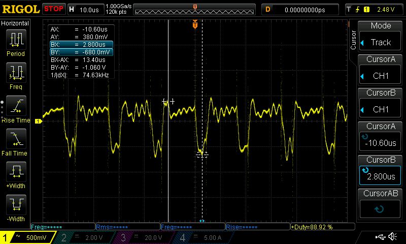
DC link voltage ripple under load#
A simple empirical rule that holds for many applications is to provide at least 20 \(\mu{}\text{F}\) of capacitance per ampere of the DC link current. Under this rule, a motor drive rated for 100 A DC requires at least 2 mF of bulk capacitance.
The DC link capacitors are usually electrolytic for reasons of cost-efficiency. One important trait of electrolytic capacitors is their limited lifetime, which is a function of several key parameters: the operating temperature, the ripple current, and the voltage. Manufacturers of electrolytic capacitors usually specify the lifetime at a specific upper-category temperature; e.g., 2500 hours at 125\(^\circ{}\text{C}\). Per Arrhenius model, the lifetime is doubled by a drop of the operating temperature by 10 kelvin; hence, a capacitor with the specified lifetime of 2500 hours at 125\(^\circ{}\text{C}\) has the expected lifetime of 10000 hours at 105\(^\circ{}C\). For a more detailed treatment of the subject, refer to “Electrolytic Capacitor Lifetime Estimation” by Albertsen, 2010.
Aside from the main bulk capacitors, it is also necessary to install low-ESR, low-ESL capacitors immediately next to each half-bridge for the suppression of high-frequency switching noise. Such high-frequency capacitors are usually either of ceramic or film type due to the strict ESR/ESL constraints. Please refer to the hardware-specific documentation for details on the recommended practices.